
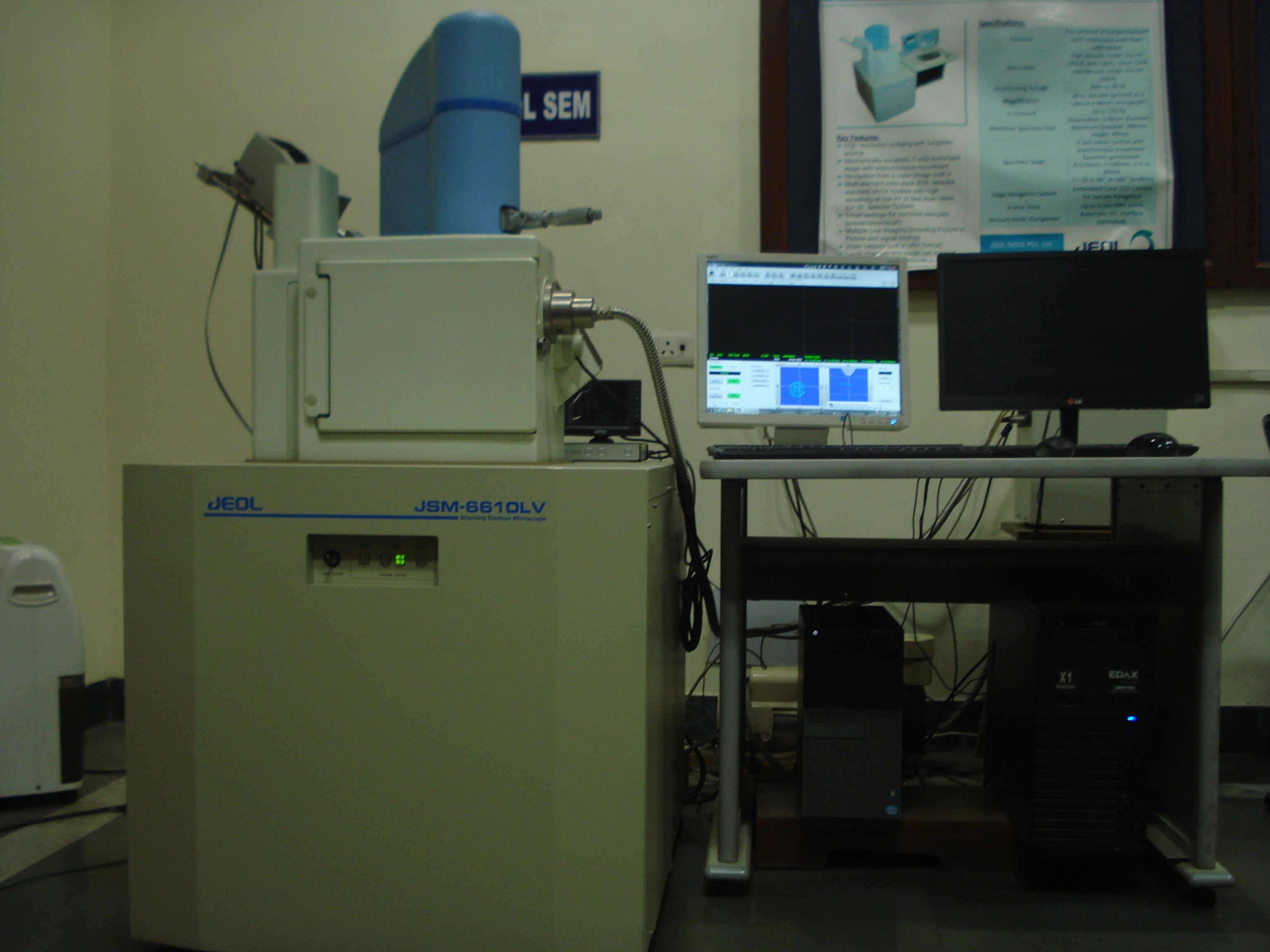
Scanning Electron Microscope (SEM)
Make: JEOL Japan Mode: JSM 6610LV
Mode: High and Low vacuum mode
Electron Sources: Tungsten or LaB 6 filament
Voltage: 1-30KV
Magnification: X5 to X 3,00,000
Resolution: 3nm with High Vacuum mode
Gold sputter coater JEC 300
Detector: Secondary, Backscattered and LN 2 free EDS detector.
Features: Surface morphology, Topography, Elemental analysis with EDS, 3D analysis with 3D software.
For any query related to the instrument,
Contact : Mr. Harsh, 9350286853
- Category Microscope Facilities
- Availability Available
- Share on
Instrument's Description
The Scanning Electron Microscope (SEM) is a type of electron microscope that images the sample surface by scanning it with high-energy beam of electrons in a raster scan pattern enabling the investigation of conductive and non-conductive materials. It offers nanometer resolution and a high signal to noise ratio. The Amatek EDS consists latest detector enables detection of elements under high resolution.
Sample Description
Because SEM utilizes vacuum conditions and uses electron beam to form an image, special sample preparations is needed as listed below:-• The sample is mounted on carbon tape that is put on the surface of the stub.
• Approximate size of the sample 1 x 1 cm (max).
• All water must be removed from the samples because the water would vaporize in the vacuum.
• Electrically conductive samples do not require any preparation before being used, however the
samples must be completely dry and free from volatile substances.
• Non-conductive samples need to be made conductive by coating the sample (using sputter
coater) with a thin layer of conductive material like Au.
Price List
| For Internal usage Per Hour | 325 |
| For Internal usage Per Sample | 100 |
| For External (Academics) usage Per Hour | 1500 |
| For External (Industries) usage Per Hour | 2500 |